| Wednesday 6 December 2017, Amsterdam #2 |
Samantha 10 December 2017 |
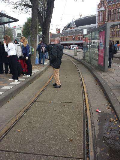
Thursday 7 December 2017, Amsterdam #3
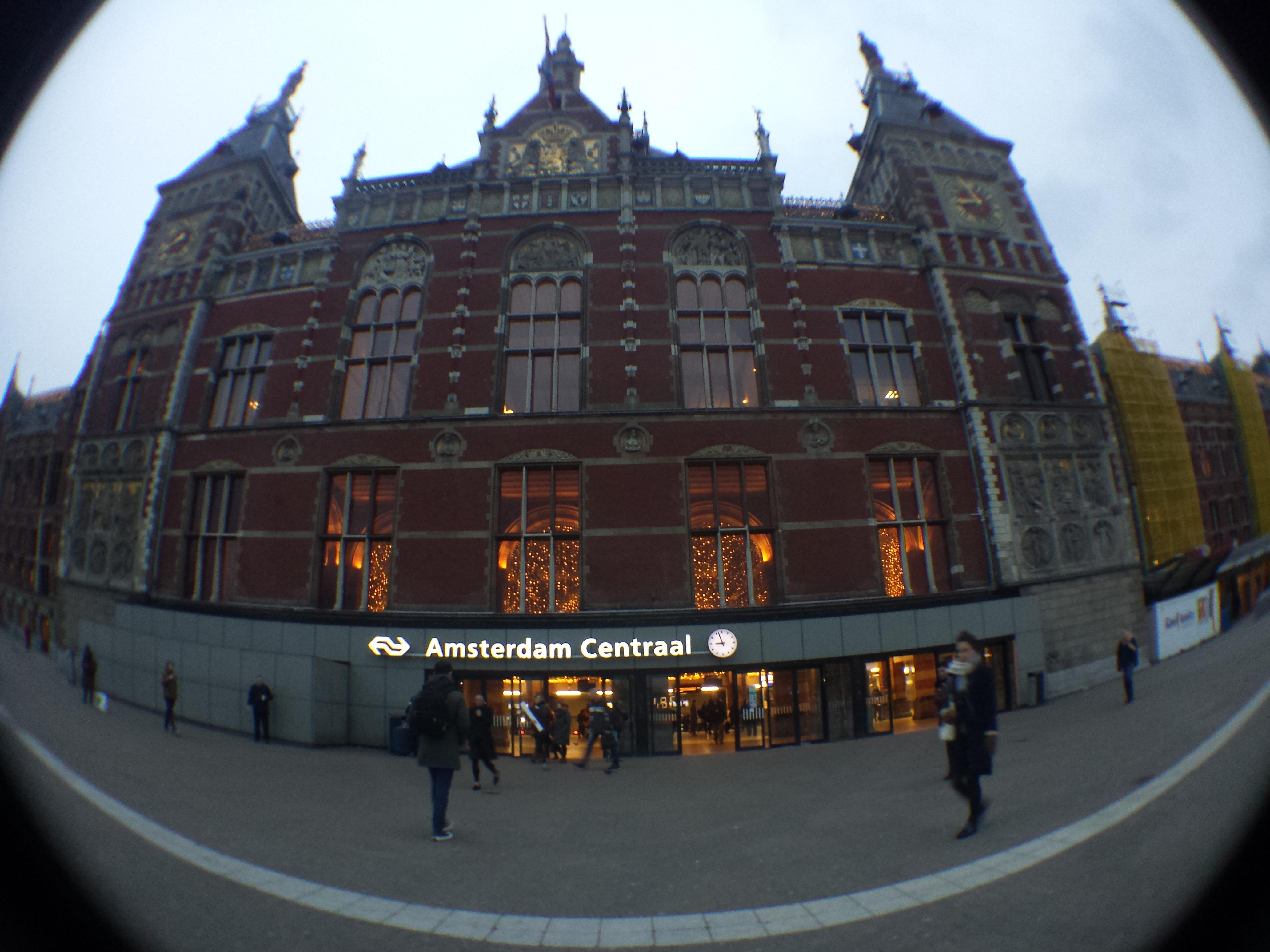
Today it is Thursday 7 December 2017 and I am on my way to Amsterdam for work for the third time. I really wanted to get on that luxurious intercity service train so I had to hurry the last moments so right now I am steaming. It was windy and the wind took my hat so I had to chase back after my hat as well.
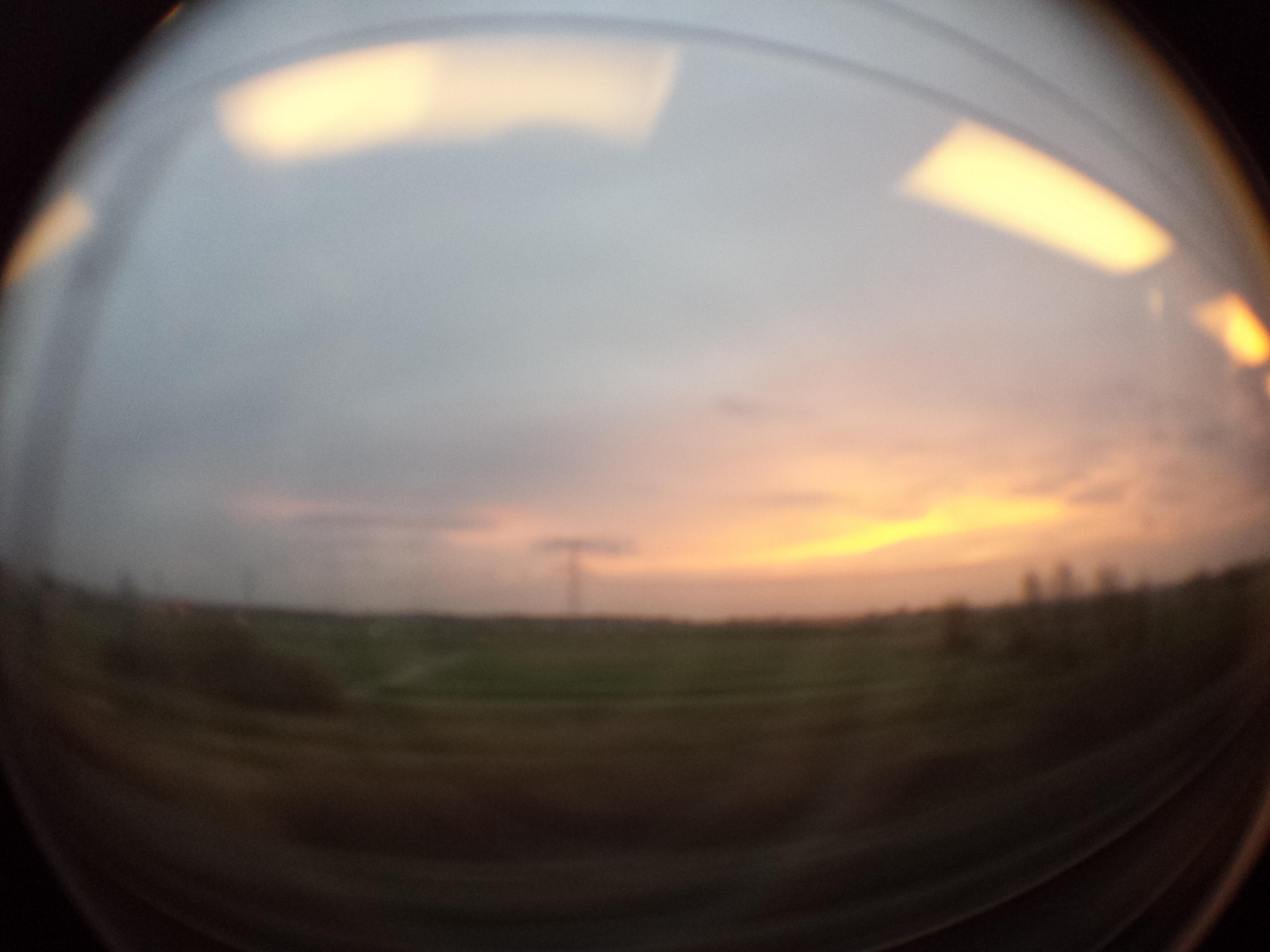
Oh well, I am on the train and I got my own private seat with my own tray to place my keyboard on. Today I also brought with me my extra lenses for the phone. I will try out some fisheye shots today.
Would it not be handy to be able to produce PCBs, Printed Circuit Boards, for various projects? For example the coaster project I am into right now. It was really frustrating making the wiring for the interior electronics for the coaster. It had been much easier if I had some of the things on a PCB. Or even better I made the PCB for the processor myself?
To find out more about this I have been searching methods of producing PCBs at home and there are plenty of methods and they are all bad or expensive.
- Traditional method. Take a clad coated with a photo-resistant material. Print the circuit layout on a transparent film and project UV light on. It is also possible to print the circuit to paper with a laser printer and then transfer the print to the clad with heat and pressure. Then the clad is developed. When that is done it is etched. Then holes are drilled. It sounds elaborate. Much chemicals and manual work.
- Then there is a method where people are sending their designs to a production house. A couple of weeks later the PCB comes back. A couple of weeks? If there are errors in the design, then new PCBs must be ordered.
- Then there is the PCB CNC milling. This sound so fantastic and there are plenty of machines out there. It is possible to make double-sided PCBs and the holes business is included. The thing though is that the machines need to be sturdy so there needs to be aluminum or steel in the construction. Many hobby level PCB mill machines are flimsy and hence those cannot achieve the necessary precision. The precision CNC mills are usually more expensive. Interestingly I found a manufacturer of CNC milling machines, Bungard, saying that PCB CNC milling is invented by persons who hate to handle chemicals. On the other hand, they also make development machines so they have a stake in the chemicals side of the business as well.
- 3D printer for PCBs with an expensive or specialist filament. These systems are so expensive they are out of reach for most hobbyists.
- Print with a silver ink:
- For this method, there is a printer from Voltera. This system does not take care of holes. The turn around time is quick but the costs of the machine are higher than many PCB CNC milling machines and they can do holes as well.
- DYI Silver Nanoparticle Ink method. Convert an inkjet printer to a silver ink printer. Soldering is difficult.
- Silver paste method. This is experimental. Print pattern on photo paper and then attach silver paste to the printed parts layer for layer, for each layer remove unwanted paste manually until there is enough conductive material. No soldering possible.
- Then there is Printem, a kind of flexible clads that you print on a standard printer and then peel off instantly. Can be soldered. Drilling?
- Conductive ink from Bare Conductive. It looks like this manufacturer got their ink working but how am I going to turn it into PCBs, no answers on that. Are there systems I could use for that? Is there a plotter to use for the Bar Conductive ink?
Perhaps I will have a look at chemicals anyway.


 I moved from Sweden to The Netherlands in 1995.
Here on this site, you find my creations because that is what I do. I create.